publications
Peer-reviewed papers grouped by year. Selected papers are marked on the homepage.
2025
- Nat. Nanotechnol.
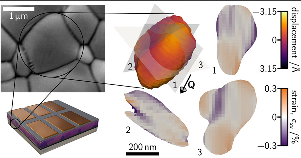
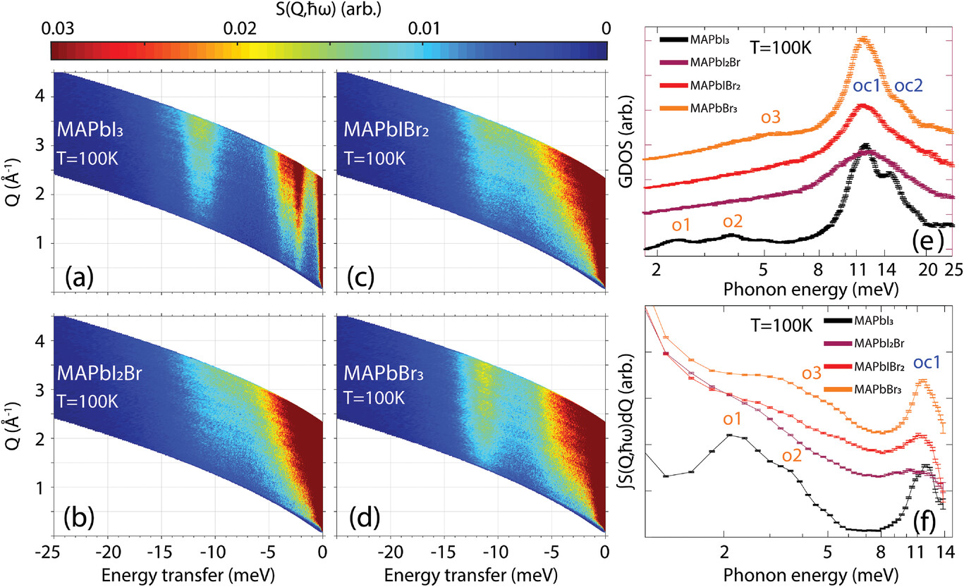
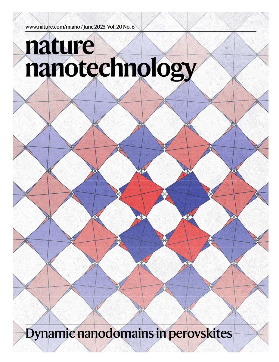 Dynamic Nanodomains Dictate Macroscopic Properties in Lead Halide PerovskitesMiloš Dubajić*, James R. Neilson, Johan Klarbring, and 31 more authorsNat. Nanotechnol., 2025Featured on the cover
Lead halide perovskites have emerged as promising materials for solar energy conversion and X-ray detection owing to their remarkable optoelectronic properties. However, the microscopic origins of their superior performance remain unclear. Here we show that low-symmetry dynamic nanodomains present in the high-symmetry average cubic phases, whose characteristics are dictated by the A-site cation, govern the macroscopic behaviour. We combine X-ray diffuse scattering, inelastic neutron spectroscopy, hyperspectral photoluminescence microscopy and machine-learning-assisted molecular dynamics simulations to directly correlate local nanoscale dynamics with macroscopic optoelectronic response. Our approach reveals that methylammonium-based perovskites form densely packed, anisotropic dynamic nanodomains with out-of-phase octahedral tilting, whereas formamidinium-based systems develop sparse, isotropic, spherical nanodomains with in-phase tilting, even when crystallography reveals cubic symmetry on average. We demonstrate that these sparsely distributed isotropic nanodomains present in formamidinium-based systems reduce electronic dynamic disorder, resulting in a beneficial optoelectronic response, thereby enhancing the performance of formamidinium-based lead halide perovskite devices. By elucidating the influence of the A-site cation on local dynamic nanodomains, and consequently, on the macroscopic properties, we propose leveraging this relationship to engineer the optoelectronic response of these materials, propelling further advancements in perovskite-based photovoltaics, optoelectronics and X-ray imaging.
- ScienceLayer-by-Layer Epitaxial Growth of Perovskite Heterostructures with Tunable Band OffsetsYang Lu‡, Young-Kwang Jung‡, Miloš Dubajić, and 22 more authorsScience, 2025
Halide perovskites exhibit superior optoelectronic properties but lack precise thickness and band offset control in heterojunctions, which is critical for modular multilayer architectures such as multiple quantum wells. We demonstrate vapor-phase, layer-by-layer heteroepitaxial growth exemplified by CsPbBr 3 deposition on single crystals of PEA 2 PbBr 4 (PEA: 2-phenylethylammonium). Angstrom-level thickness control and subangstrom smooth layers enable quantum-confined photoluminescence of CsPbBr 3 from monolayer, bilayer, and through to bulk. The interfacial structure controls the electronic structure from a Cs‒PEA-terminated interface (type II heterojunction) to a PEA‒PEA-terminated interface (type I heterojunction), with a layer-tunable band offset shift exceeding 0.5 electron volts. Electron transfer from CsPbBr 3 to PEA 2 PbBr 4 for a type II Cs‒PEA heterojunction results in delayed electron-hole recombination beyond 10 microseconds. Precise quantum confinement control and large band offset tunability unlock perovskite heterojunctions as platforms for scalable, superlattice-based optoelectronic applications.
- PRX EnergyAccurate Determination of Phonon Lifetimes from the Spectral DomainMiloš Dubajić*, Andreas Pusch, Michael P. Nielsen, and 1 more authorPRX Energy, 2025
Concerningly, numerous incorrect expressions for extracting phonon lifetimes from spectroscopic linewidths remain prevalent in the literature, resulting in misinterpretation of experimental data. This has significant consequences in the broader energy materials field, where erroneous lifetimes risk misinforming materials design and device modeling. We outline the origin of this ambiguity, provide historical context on how this error has propagated, and present the correct formula. In addition, we highlight a frequently overlooked source of error: the contribution of phase relaxation to spectral broadening. A unified approach enables fair comparison of values obtained from different spectroscopic methods, accurate benchmarking against first-principles calculations, and, most importantly, precise determination of macroscopic physical properties derived from phonon lifetime measurements.
- Nat. Rev. Methods Primers
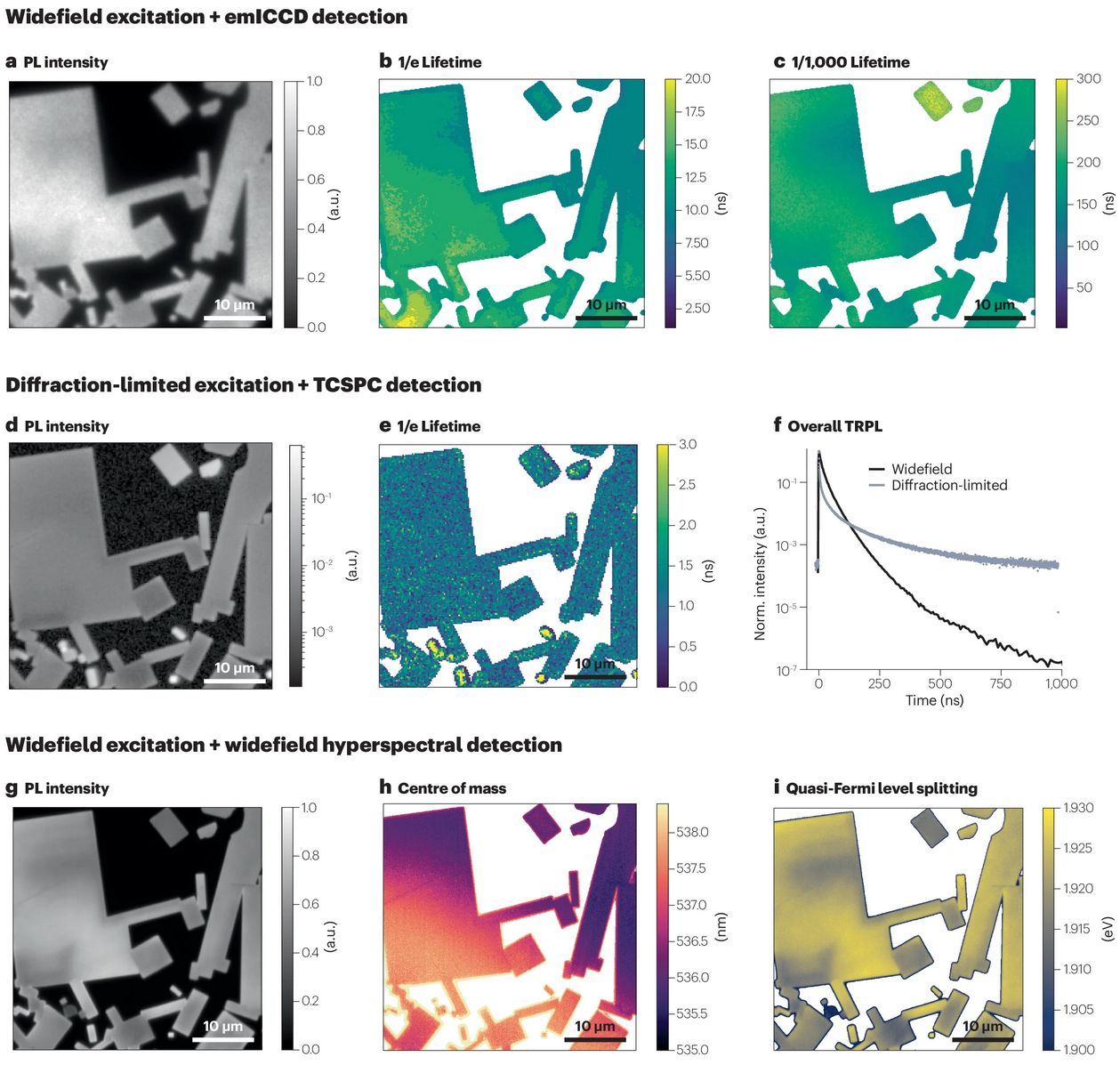 Photoluminescence Microscopy of Optoelectronic MaterialsZimu Wei, Miloš Dubajić, Cullen Chosy, and 2 more authorsNat. Rev. Methods Primers, 2025
Photoluminescence (PL) microscopy is a technique for mapping the spatial distribution of optical and electronic properties in optoelectronic (OE) materials, including silicon, III–V and organic semiconductors, halide perovskites and quantum dots. This Primer provides an overview of the foundational principles and methods of PL microscopy, highlighting how different microscopy configurations can reveal unique insights into the photophysical behaviours of OE materials and the importance of selecting appropriate set-ups for accurate analysis. Key topics include acquisition modes such as widefield and confocal scanning, along with time-resolved and spectrally resolved PL techniques. Practical guidance on experimental set-up, data acquisition and analytical approaches is provided, addressing common challenges and limitations. Finally, emerging applications, solutions to typical issues and potential advancements in PL imaging are discussed, with the goal of supporting the optimization of next-generation OE materials and devices.
- ACS Nano
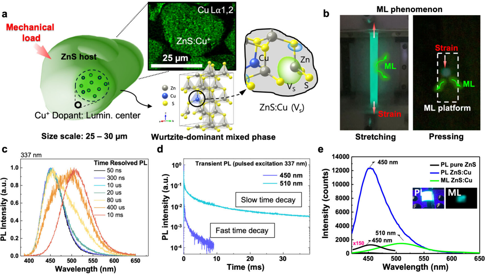 Defect-Localized Mechanoluminescence Model in Copper-Doped Zinc SulfideHong In Jeong‡, Miloš Dubajić‡, Cheong Beom Lee, and 11 more authorsACS Nano, 2025
Doped zinc sulfide microparticles exhibit the ability to mechanically tune their luminescence properties, making them promising candidates for mechanoluminescence materials that can be used in a diverse array of next-generation optoelectronics. However, their mechanism remains unclear and is often attributed to intricate analytical misinterpretations, which impede the development of a fundamental theory for improving this innovative technology. Here, we visualize the mechanoluminescence dynamics of copper-doped zinc sulfide through a hybrid technique in which structural-optical properties are correlated at an identical sample level. These results reveal that Cu defects are much more susceptible to lattice distortion when strain is applied to the global structure, which locally populates charge carriers to the electronic states responsible for mechanoluminescence. This promotes the mechanoluminescence emission from localized defect sites rather than from the global ZnS lattice. Our defect-localized mechanoluminescence model, triggered by an elastic strain, provides fundamental insights into this long-standing enigma, yielding implications for the design of high-performance materials in next-generation applications.
- Nat. Nanotechnol.
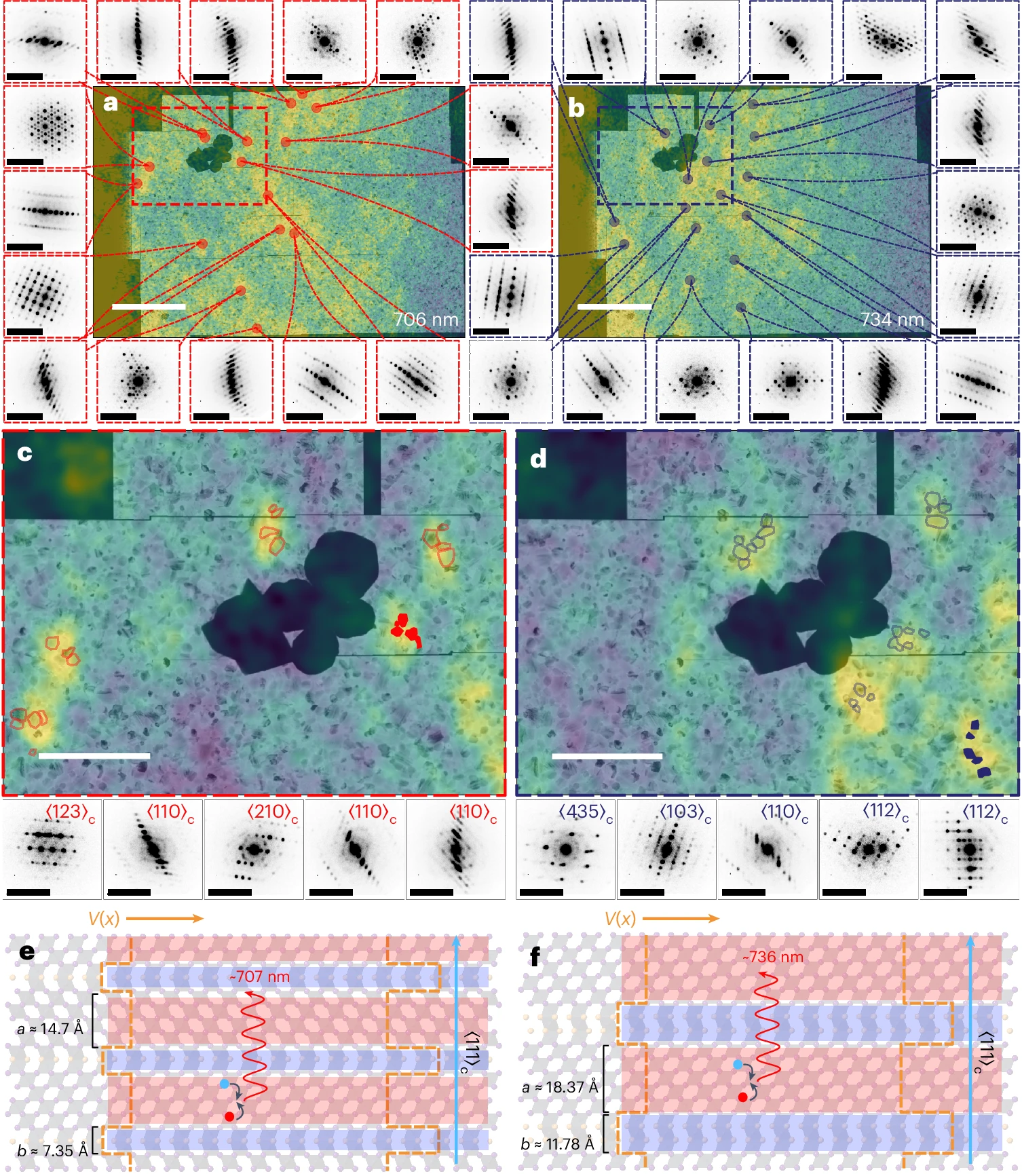 Picosecond Quantum Transients in Halide Perovskite Nanodomain SuperlatticesDengyang Guo, Thomas A. Selby, Simon Kahmann, and 21 more authorsNat. Nanotechnol., 2025
The high optoelectronic quality of halide perovskites makes them suitable for use in optoelectronic devices and, recently, in emerging quantum emission applications. Advancements in perovskite nanomaterials have led to the discovery of processes in which luminescence decay times are below 100 picoseconds, stimulating the exploration of even faster radiative rates for advanced quantum applications, which have only been realized in III–V materials grown using costly epitaxial growth methods. Here we discovered ultrafast quantum transients with timescales of around two picoseconds at low temperature in bulk formamidinium lead iodide films grown via scalable solution or vapour approaches. Using a multimodal strategy, combining ultrafast spectroscopy, optical and electron microscopy, we show that these transients originate from quantum tunnelling in nanodomain superlattices. The outcome of the transient decays, that is, photoluminescence, mirrors the photoabsorption of the states, with an ultranarrow linewidth at low temperature that can reach <2 nm ( 4 meV). Localized correlation of the emission and structure reveals that the nanodomain superlattices are formed by alternating ordered layers of corner-sharing and face-sharing octahedra. This discovery opens new applications leveraging intrinsic quantum properties and demonstrates powerful multimodal approaches for quantum investigations.
- Nat. Commun.
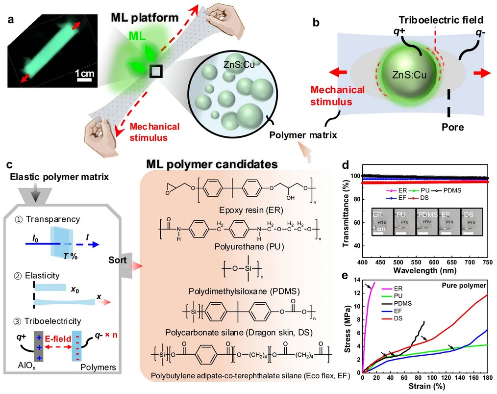 Super-Elastic and Negative Triboelectric Polymer Matrix for High-Performance Mechanoluminescent PlatformsHong In Jeong, Hye Sung Jung, Miloš Dubajić, and 12 more authorsNat. Commun., 2025
Mechanoluminescence platforms, combining phosphors with elastic polymer matrix, have emerged in smart wearable technology due to their superior elasticity and mechanically driven luminescent properties. However, their luminescence performance often deteriorates under extreme elastic conditions owing to a misinterpretation of polymer matrix behavior. Here, we unveil the role of the polymer matrices in mechanoluminescence through an interface-triboelectric effect driven by elasticity, achieving both high elasticity and brightness. By investigating interactions between elastic polymers and copper doped zinc sulfide microparticles, we reveal that elasticity significantly governed triboelectric effects for mechanoluminescence. In particular, high negative triboelectricity emerged as the key to overcoming poor triboelectric effect in extreme elastic conditions. This led to the discovery of polybutylene adipate-co-terephthalate silane and polycarbonate silane, achieving remarkable elasticity over 100% and a brightness of 139 cd/m2. These findings offer fundamental insights to select the optimal polymer matrix based on systematic parameters for various smart wearable applications.
- J. Phys. Chem. Lett.
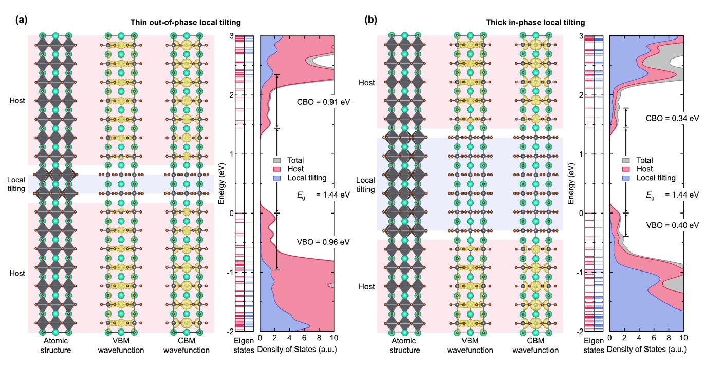 Electronic Consequences of the Formation of Local Tilting in Halide PerovskitesYoung-Kwang Jung, Miloš Dubajić, and Samuel D. StranksJ. Phys. Chem. Lett., 2025
Complex structural dynamics in halide perovskites have attracted researchers in the field of perovskite optoelectronics. Although state-of-the-art experimental and theoretical techniques have disclosed the dynamic nature of local tilting in halide perovskites, how such local tilting influences the physical properties of these materials is still poorly understood. In this study, we model confined local tilting within a cubic halide perovskite CsPbBr3 and reveal the electronic consequences of the local tilting, employing density functional theory. Our calculations confirm that the locally tilted layers have larger band gaps than the host cubic lattice, where no charge trapping levels are introduced by them. The degree of local band gap fluctuation is predicted to depend significantly on the geometry of the locally tilted domains. We conclude that local tilting will act as dynamic charge-blocking barriers, which impact carrier dynamics in perovskite optoelectronic devices.
- J. Am. Chem. Soc.
 Molecular Engineering of Interlayer Exciton Delocalization in 2D PerovskitesYorrick Boeije, Fabian Lie, Miloš Dubajić, and 20 more authorsJ. Am. Chem. Soc., 2025
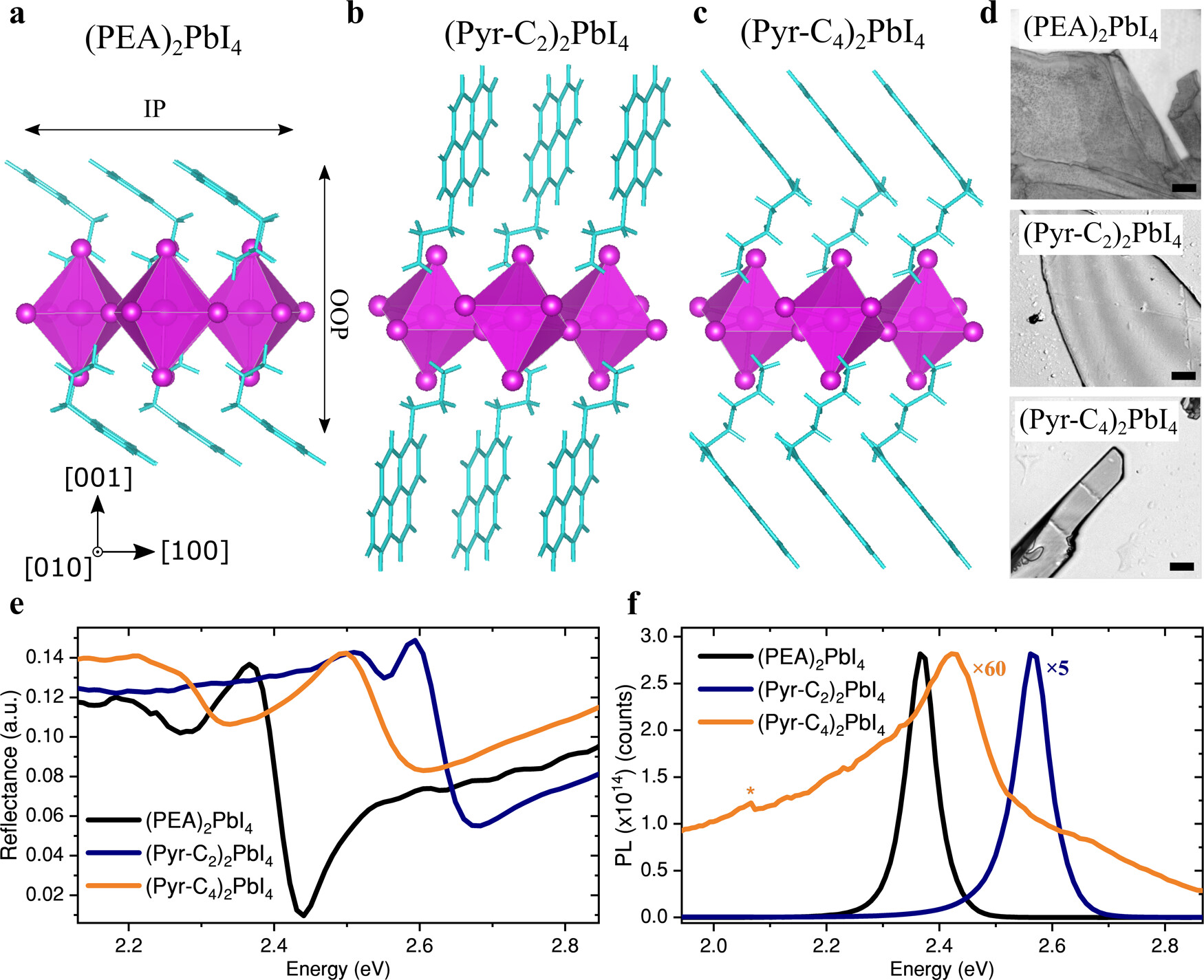
In recent years, significant progress has been made in improving the stability, photocurrent efficiency and charge transport properties of 2D hybrid perovskites, making them increasingly relevant for optoelectronic devices. Although these layered systems are typically considered quantum wells due to carrier confinement, an emerging strategy is to generate new perovskite functionalities with π-conjugated electroactive cores as spacer molecules, which introduce electronic coupling between the inorganic metal-halide and organic sublattices. Realizing these functionalities requires an understanding of how this coupling is achieved and how it affects exciton behavior. Using first-principles modeling and single-crystal optical spectroscopy, we find that the linker length (Cx, where x = 2 or 4) controls the inorganic-organic electronic coupling and, therefore, the exciton properties of pyrene-alkylammonium (Pyr-Cx)-based electroactive 2D perovskites. Whereas both (Pyr-C2)2PbI4 and (Pyr-C4)2PbI4 incorporate the π-conjugated core, only the latter has electroactive characteristics, as the longer linker length (x = 4) allows favorable π-π stacking that, together with energy alignment of organic and inorganic orbitals, results in interlayer organic-inorganic hybridization. This tailored hybrid coupling induces substantial exciton "leakage" through multiple PbI42- layers, enabling efficient interlayer exciton transport. By contrast, due to a type-I band alignment and orthogonal orientation of the π-systems with respect to the PbI42- layers in (Pyr-C2)2PbI4, the interlayer hybridization is lost, resulting in traditional quantum well properties. This study reveals new molecular engineering design principles to control excitons in 2D perovskites, emphasizing the importance of active π-core orientation and energetic band alignment─marking a critical step toward harnessing active organic cations in perovskite optoelectronics.
- J. Am. Chem. Soc.
 Light-Driven Intra-Octahedral Halide Isomerisation in Two-Dimensional Mixed-Halide PerovskitesWenxin Mao, Enamul Haque, Stephanie A. Bird, and 18 more authorsJ. Am. Chem. Soc., 2025
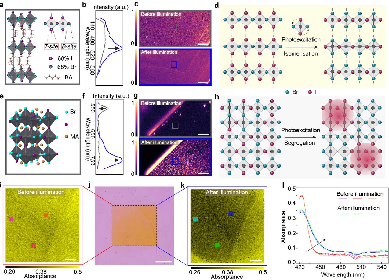
Two-dimensional metal halide perovskites are emerging materials for quantum light emission and neuromorphic computing owing to their quantum-confined structures and tunable optoelectronic properties. Beyond structural dimensionality, the presence of multiple crystallographically distinct halide sites within a single metal halide octahedron presents a unique opportunity to engineer functionality at the subunit-cell level. Here, we report a light-driven, reversible halide-ion isomerization in single-crystalline BA2PbBrxI4-x (BA = butylammonium, x = 1-3), where ions switch between distinct local configurations within individual PbX64- octahedra, without long-range migration or macroscopic phase segregation. Through a combination of hyperspectral imaging, in situ X-ray diffraction, and first-principles calculations, we demonstrate that this intraoctahedral halide site switching modulates the optical bandgap by ∼0.1 eV and enables an estimated reversible electronic bandgap shift of up to ∼0.5 eV. Density functional theory reveals that these changes stem from a redistribution of valence band character, effectively creating chemically distinct optoelectronic isomers that can be activated by light. These results uncover a mechanism of structurally encoded, site-selective photoisomerization in 2D perovskites, offering a new strategy for reconfigurable optoelectronic devices, nonvolatile optical memory, and quantum photonics.
- Adv. Mater.
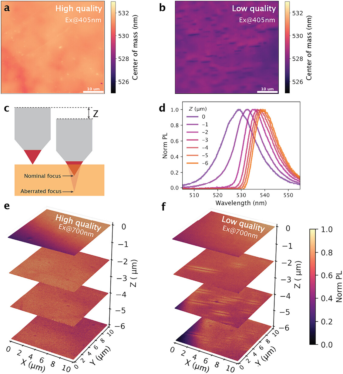 Carrier Diffusion Links Single-Crystal Quality and Photoluminescence in Halide Perovskite Radiation DetectorsZimu Wei, Khasim Saheb Bayikadi, Capucine Mamak, and 5 more authorsAdv. Mater., 2025
Halide perovskites have emerged as promising materials for next‐generation radiation detectors, echoing their transformative impact on photovoltaics. Due to the long penetration depths of X‐rays and γ‐rays, thick single crystals are required to sufficiently attenuate the radiation, making bulk crystal quality critical for device performance. Photoluminescence properties, particularly long lifetimes and redshifted emission peaks, are commonly used as proxies for identifying high‐quality CsPbBr 3 crystals for high‐performance detectors, yet the physical origin of this correlation remains unclear. Here, complementary photoluminescence techniques with a full‐spectrum fit are combined to reveal the importance of vertical diffusion in governing photoluminescence response, ultimately shaping detector performance. High‐quality crystals exhibit larger vertical diffusion coefficients (up to 0.65 cm 2 s −1 ) and lower recombination rates (down to 1.1 × 10 6 s −1 ), leading to diffusion lengths up to 5 times greater than those in low‐quality crystals. Using one‐ and two‐photon photoluminescence microscopy, microscale defects are further visualized, with suppressed redshift and distributions throughout the bulk, in low‐quality crystals. Two‐photon diffusion mapping directly reveals how these defects hinder carrier transport. These findings establish a direct link between photoluminescence and carrier diffusion, providing a quantitative framework that connects crystal quality to charge transport and device performance in perovskite radiation detectors.
2024
- Adv. Funct. Mater.
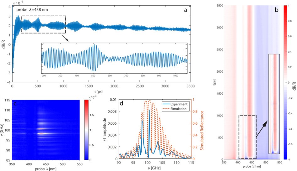 Long-Lived Acoustic Phonon and Carrier Dynamics in III–V Adiabatic CavitiesMuhammad Hanif, Miloš Dubajić*, Sujakala J. Sreerag, and 4 more authorsAdv. Funct. Mater., 2024
Evidence of strongly confined coherent acoustic phonons inside high quality factor phononic cavities that exhibit tailored phonon potentials is provided. Using GaAs/AlAs quasiperiodic superlattices, functional phonon potentials are realized by adiabatically changing the layer thicknesses along the growth direction. Room temperature ultrafast vibrational spectroscopy reveals discrete phonon modes with frequencies in the range of ≈96–101 GHz. Additionally, it is confirmed that phononic cavities impact the energy loss rate of the photoexcited carriers, as evidenced by time‐resolved photoluminescence measurements. These results highlight the potential of concurrently engineering optoelectronic and phononic properties for a range of novel applications.
- Nature
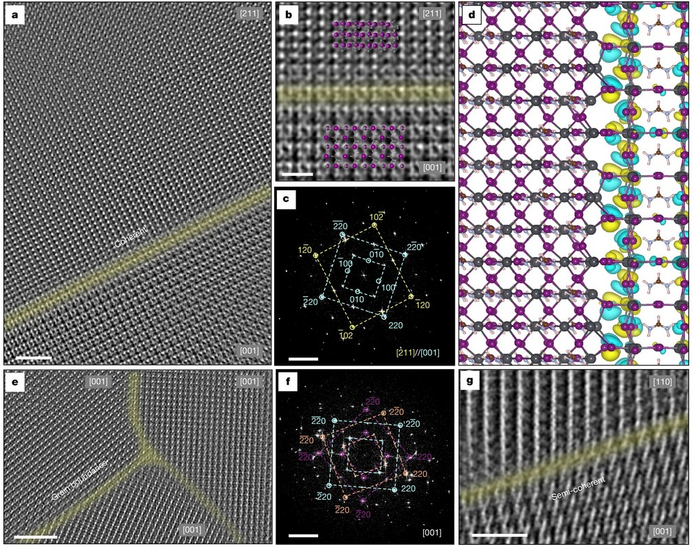 Coherent Growth of High-Miller-Index Facets Enhances Perovskite Solar CellsShunde Li, Yun Xiao, Rui Su, and 36 more authorsNature, 2024
 - Nat. Energy
 The Impact of Interfacial Quality and Nanoscale Performance Disorder on the Stability of Alloyed Perovskite Solar CellsKyle Frohna, Cullen Chosy, Amran Al-Ashouri, and 12 more authorsNat. Energy, 2024
Microscopy provides a proxy for assessing the operation of perovskite solar cells, yet most works in the literature have focused on bare perovskite thin films, missing charge transport and recombination losses present in full devices. Here we demonstrate a multimodal operando microscopy toolkit to measure and spatially correlate nanoscale charge transport losses, recombination losses and chemical composition. By applying this toolkit to the same scan areas of state-of-the-art, alloyed perovskite cells before and after extended operation, we show that devices with the highest macroscopic performance have the lowest initial performance spatial heterogeneity—a crucial link that is missed in conventional microscopy. We show that engineering stable interfaces is critical to achieving robust devices. Once the interfaces are stabilized, we show that compositional engineering to homogenize charge extraction and to minimize variations in local power conversion efficiency is critical to improve performance and stability. We find that in our device space, perovskites can tolerate spatial disorder in chemistry, but not charge extraction.
- ACS Energy Lett.
 Strain Heterogeneity and Extended Defects in Halide Perovskite DevicesKieran W. P. Orr, Jiecheng Diao, Krishanu Dey, and 14 more authorsACS Energy Lett., 2024
Strain is an important property in halide perovskite semiconductors used for optoelectronic applications because of its ability to influence device efficiency and stability. However, descriptions of strain in these materials are generally limited to bulk averages of bare films, which miss important property-determining heterogeneities that occur on the nanoscale and at interfaces in multilayer device stacks. Here, we present three-dimensional nanoscale strain mapping using Bragg coherent diffraction imaging of individual grains in Cs0.1FA0.9Pb(I0.95Br0.05)3 and Cs0.15FA0.85SnI3 (FA = formamidinium) halide perovskite absorbers buried in full solar cell devices. We discover large local strains and striking intragrain and grain-to-grain strain heterogeneity, identifying distinct islands of tensile and compressive strain inside grains. Additionally, we directly image dislocations with surprising regularity in Cs0.15FA0.85SnI3 grains and find evidence for dislocation-induced antiphase boundary formation. Our results shine a rare light on the nanoscale strains in these materials in their technologically relevant device setting.
- Adv. Mater.
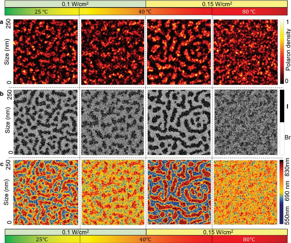 Thermal-Disorder-Induced Strain and Carrier Localisation Activate Reverse Halide SegregationNursultan Mussakhanuly, Arman Mahboubi Soufiani, Stefano Bernardi, and 14 more authorsAdv. Mater., 2024
The reversal of halide ions is studied under various conditions. However, the underlying mechanism of heat‐induced reversal remains unclear. This work finds that dynamic disorder‐induced localization of self‐trapped polarons and thermal disorder‐induced strain (TDIS) can be co‐acting drivers of reverse segregation. Localization of polarons results in an order of magnitude decrease in excess carrier density (polaron population), causing a reduced impact of the light‐induced strain (LIS – responsible for segregation) on the perovskite framework. Meanwhile, exposing the lattice to TDIS exceeding the LIS can eliminate the photoexcitation‐induced strain gradient, as thermal fluctuations of the lattice can mask the LIS strain. Under continuous 0.1 W cm⁻2 illumination (upon segregation), the strain disorder is estimated to be 0.14%, while at 80 °C under dark conditions, the strain is 0.23%. However, in situ heating of the segregated film to 80 °C under continuous illumination (upon reversal) increases the total strain disorder to 0.25%, where TDIS is likely to have a dominant contribution. Therefore, the contribution of entropy to the system’s free energy is likely to dominate, respectively. Various temperature‐dependent in situ measurements and simulations further support the results. These findings highlight the importance of strain homogenization for designing stable perovskites under real‐world operating conditions.
- Adv. Mater.
 Imaging Light-Induced Migration of Dislocations in Halide Perovskites with 3D Nanoscale Strain MappingKieran W. P. Orr, Jiecheng Diao, Muhammad Naufal Lintangpradipto, and 14 more authorsAdv. Mater., 2024
In recent years, halide perovskite materials have been used to make high‐performance solar cells and light‐emitting devices. However, material defects still limit device performance and stability. Here, synchrotron‐based Bragg coherent diffraction imaging is used to visualize nanoscale strain fields, such as those local to defects, in halide perovskite microcrystals. Significant strain heterogeneity within MAPbBr3 (MA = CH3NH3+) crystals is found in spite of their high optoelectronic quality, and both 〈100〉 and 〈110〉 edge dislocations are identified through analysis of their local strain fields. By imaging these defects and strain fields in situ under continuous illumination, dramatic light‐induced dislocation migration across hundreds of nanometers is uncovered. Further, by selectively studying crystals that are damaged by the X‐ray beam, large dislocation densities and increased nanoscale strains are correlated with material degradation and substantially altered optoelectronic properties assessed using photoluminescence microscopy measurements. These results demonstrate the dynamic nature of extended defects and strain in halide perovskites, which will have important consequences for device performance and operational stability.
2023
- SmallDynamic Local Structure in Caesium Lead Iodide, Spatial Correlation and Transient DomainsWilliam J. Baldwin, Xia Liang, Johan Klarbring, and 8 more authorsSmall, 2023
Metal halide perovskites are multifunctional semiconductors with tunable structures and properties. They are highly dynamic crystals with complex octahedral tilting patterns and strongly anharmonic atomic behavior. In the higher temperature, higher symmetry phases of these materials, several complex structural features are observed. The local structure can differ greatly from the average structure and there is evidence that dynamic 2D structures of correlated octahedral motion form. An understanding of the underlying complex atomistic dynamics is, however, still lacking. In this work, the local structure of the inorganic perovskite CsPbI3 is investigated using a new machine learning force field based on the atomic cluster expansion framework. Through analysis of the temporal and spatial correlation observed during large‐scale simulations, it is revealed that the low frequency motion of octahedral tilts implies a double‐well effective potential landscape, even well into the cubic phase. Moreover, dynamic local regions of lower symmetry are present within both higher symmetry phases. These regions are planar and the length and timescales of the motion are reported. Finally, the spatial arrangement of these features and their interactions are investigated and visualized, providing a comprehensive picture of local structure in the higher symmetry phases.
- Adv. Energy Mater.
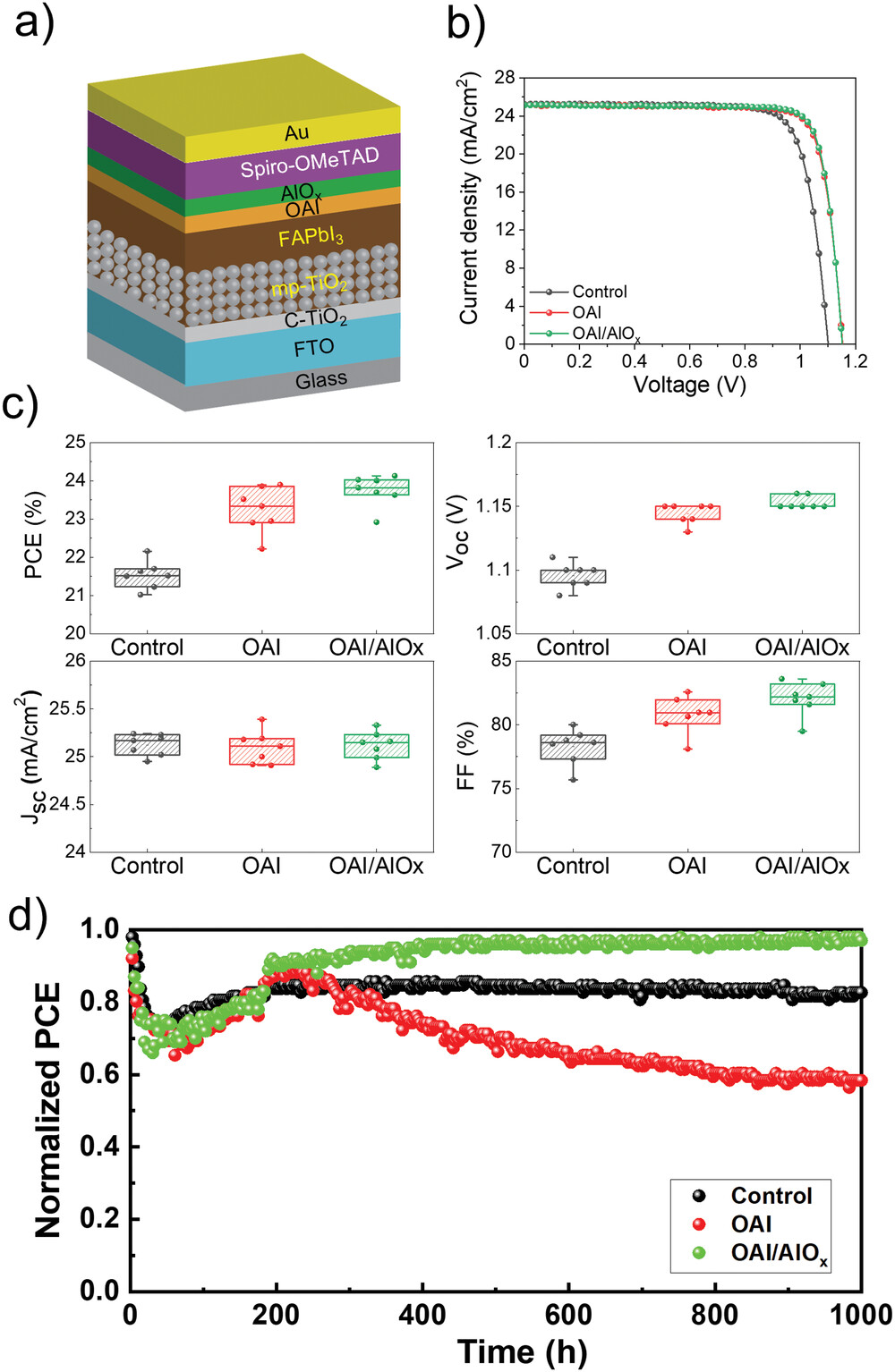 Synergetic Effect of Aluminium Oxide and Organic Halide Salts on Two-Dimensional Perovskite Layer Formation and Stability Enhancement of Perovskite Solar CellsEunyoung Choi, Jin‐Won Lee, Miguel Anaya, and 14 more authorsAdv. Energy Mater., 2023
Long‐chain organic halide salts are widely used in perovskite‐based optoelectronic devices for surface passivation owing to their capability to interact with the surface defects of perovskites. Here, aluminum oxide (AlOx) is introduced via atomic layer deposition onto octylammonium iodide (OAI) to exploit the benefits of organic halide salts without generating undesired defects. The devices incorporating AlOx on OAI‐treated perovskite (OAI/AlOx) show enhancement in both device performance and photo‐stability compared to those with only treatment. A diffusion of aluminum from AlOx into the perovskite through surface characterization contributes to a uniform photo‐generated carrier transport in both the surface and the bulk of the perovskite absorber. In addition, it is revealed that light‐induced two‐dimensional perovskite formation on OAI/AlOx. This may be ascribed to preventing the loss of OA cations due to the presence of AlOx, leading to a decrease in the number of iodine anions which suppresses the light‐induced degradation of corresponding devices. Consequently, the devices show over 24% efficiency and retain their efficiency over 1000 hours under continuous light illumination.
2022
- Small
 Anomalous Structural Evolution and Glassy Lattice in Mixed-Halide Hybrid PerovskitesShamim Shahrokhi‡, Miloš Dubajić‡, Zhi‐Zhan Dai, and 19 more authorsSmall, 2022
Hybrid halide perovskites have emerged as highly promising photovoltaic materials because of their exceptional optoelectronic properties, which are often optimized via compositional engineering like mixing halides. It is well established that hybrid perovskites undergo a series of structural phase transitions as temperature varies. In this work, the authors find that phase transitions are substantially suppressed in mixed‐halide hybrid perovskite single crystals of MAPbI3‐xBrx (MA = CH3NH3+ and x = 1 or 2) using a complementary suite of diffraction and spectroscopic techniques. Furthermore, as a general behavior, multiple crystallographic phases coexist in mixed‐halide perovskites over a wide temperature range, and a slightly distorted monoclinic phase, hitherto unreported for hybrid perovskites, is dominant at temperatures above 100 K. The anomalous structural evolution is correlated with the glassy behavior of organic cations and optical phonons in mixed‐halide perovskites. This work demonstrates the complex interplay between composition engineering and lattice dynamics in hybrid perovskites, shedding new light on their unique properties.
2021
- Prog. Photovolt.
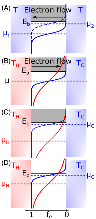 Optoelectronic Reciprocity in Hot-Carrier Solar Cells with Ideal Energy-Selective ContactsAndreas Pusch, Miloš Dubajić, Michael P. Nielsen, and 3 more authorsProg. Photovolt. Res. Appl., 2021
Hot carrier solar cells promise theoretical power conversion efficiencies far beyond the single junction limit. However, practical implementations of hot carrier solar cells have lagged far behind those theoretical predictions. Reciprocity relations for electroluminescence from conventional single junction solar cells have been extremely helpful in driving their efficiency ever closer to the theoretical limits. In this work, we discuss how the signatures of a functioning hot carrier device should manifest experimentally when driven in reverse, that is, in electroluminescent mode. Hot carrier properties lead to deviations of the dark I–V from the Shockley diode equation that is typical for conventional single junction solar cells. These deviations are directly linked to an increase in temperature of the carriers and therefore the temperature measured from electroluminescence spectra. We also elucidate how the behaviour of hot carrier solar cells in the dark depends on whether Auger processes play a significant role, revealing a stark contrast between the regime of negligible Auger recombination (carrier conservation model) and dominant Auger recombination (impact ionisation model) for hot carrier solar cells.
2020
- Electron. Struct.
 Hafnium and Zirconium Nitrides with Rock-Salt and Th3P4 Structures, Electronic and Phonon Band-Structure Calculations to Examine Hot-Carrier Solar Cell and Thermoelectric PropertiesBharat Thapa, Robert Patterson, Miloš Dubajić, and 2 more authorsElectron. Struct., 2020
Hafnium and zirconium mononitrides (HfN and ZrN) have been of interest for the hot carrier solar cell (HCSC) concept as a bulk absorber material and in thermoelectric power generation as a superlattice structure. Slowed hot carrier (HC) cooling is a fundamental requirement in an HCSC device because the carriers must be collected at high energy levels via energy selective contacts before they cool down to the band edges. However, achieving longer thermalization time is challenging in bulk materials. Here, we have calculated electronic and phonon properties of rock-salt HfN and ZrN and the nitrogen-rich thorium phosphide (Th 3 P 4 ) structures: c-Hf 3 N 4 and c-Zr 3 N 4 using a first principle density functional theory method. Electronic and phonon band structures of alloyed Hf and Zr in the nitrogen-rich phases are presented for the first time. Our calculations show that the mononitrides of Hf and Zr have wide optical phonon (OP) to acoustic phonon (AP) band gap and simultaneous smaller OP dispersion that have the potential to slow down the HCs cooling rates, making them suitable for an HCSC absorber. Further, the results provide a first step towards exploring both HCSC and thermoelectric properties in metal/semiconductor superlattice structure of nitrides of Hf and Zr only.
2018
- Opt. Quantum Electron.
 Optimisation of Cubic GaN/AlGaN Quantum-Cascade Structures for Negative Refraction in the THz Spectral RangeMiloš Dubajić, Aleksandar Daničić, Nikola Vuković, and 2 more authorsOpt. Quantum Electron., 2018
In this work we theoretically investigate a possibility to use cubic nitride based multi-layer periodic nanostructure as a semiconductor metamaterial. The structure design is based on an active region of a quantum cascade laser optimized to achieve optical gain in the Terahertz (THz) spectral range. In particular, we test the GaN/AlGaN quantum well configurations, which should exhibit important advantages compared to GaAs-based structures, namely room temperature operation without the assistance of magnetic field and lower doping densities. Our numerical rate-equations model is solved self-consistently and it takes into account electron-longitudinal optical phonon scattering between all the relevant states among the adjacent periods of the structure. A global optimization routine, specifically genetic algorithm is then used to generate new gain-optimized structures. This work confirms the advantages of cubic GaN designs over GaAs ones, namely feasibility of negative refraction at room temperature without the assistance of magnetic field while keeping the doping densities of the same order of magnitude.